


The mobile phone has become an essential tool in everyday life. It's even used for accessing the Internet and managing databases. Mobile phones have revolutionized the conventional concept of a telephone and are continuing to develop by leaps and bounds every day. We are proud to provide resin for use in these exciting technological wonders.
Electronic Material Resins
Rediscover resin as a material for electronics
Phenolic resins have been used widely not only in ever-popular mobile phones, but also in the manufacturing of semiconductors, which play a central role as the "brains" of PCs and LCD TVs. As a frontrunner in the field, we established a "selective synthesis technology" for selectively synthesizing a phenolic derivative*1 using an ion exchange resin.*2 This technology has been highly regarded not only in the world of industry, but also in the academic field. This technology, now one of our core technologies, allows us to manufacture phenolic derivatives (ballast material). Phenolic derivatives are the raw materials for photo-resists (photosensitive resins), which are essential in the making of semiconductor circuits. Furthermore, we have also succeeded in developing high-purity phenolic resins, vital to the manufacturing of photo-resists. These resins are mainly used in the manufacturing of semiconductor integrated circuits, printed circuit boards, and flat panel displays, and as such are important materials for IT companies. We provide various phenolic derivatives and high-purity phenolic resins to suit the unique needs of our customers.
- *1: Resin has a handle that traps the ions.
- *2: Compounds controlled a molecular structure made from phenols.
Photo-resist disappears during the manufacturing process
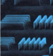
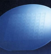
The technique called "photolithography" is one application of the principle of photography. A semiconductor's electronic circuit is made using this technique to imprint a microscopic circuit pattern. There are four processes in semiconductor manufacturing.
(1) Silicon Wafer Manufacturing(2) Photomask Manufacturing(3) Wafer Treatment
(4) Assembly Photo-resist is a photosensitizing agent used in wafer treatment for imprinting a complex circuit pattern on a silicon chip that is only a few millimeters square. Phenolic derivatives and high-purity phenolic resins are used as the raw materials for this photo-resist. As shown here, the photo-resist disappears during the manufacturing process, and does not remain on the electronic circuit itself. It's an indispensable material in electronics manufacturing.
Process of treating a silicon wafer
All semiconductors are manufactured through a combination of the following processes:
- Oxide film creation: An insulating film of silicon dioxide is formed by heating the highly polished surface of a silicon wafer measuring approximately 0.5 mm thick.
- Application of photo-resist: A spin coater rotates the silicon wafer as photo-resist is applied to its surface by centrifugal force. A light is shined on the silicon wafer through a glass substrate (photo-mask) that bears an electronic circuit pattern. The photo-resist is exposed only where the circuit pattern has been drawn.
- Silicon wafer development: The silicon wafer is developed and the photo-resist is washed away in the exposed areas, revealing the silicon dioxide layer.
- Etching: The revealed areas are carved out further via etching. The transfer of the image to the silicon wafer is complete after the remaining photo-resist is removed.
- Formation of film: an insulating film of silicon dioxide is once again formed.
With the progress of the electronics industry

Photo-resist also evolves with time. For example, the wavelength of light used is becoming shorter and shorter. Circuit miniaturization has progressed remarkably thanks to this shortened wavelength, making it possible to manufacture even more advanced electronics. Just think: a short time ago, a PC's hard disk was rather large. Now it has been miniaturized down to only a few centimeters. This miniaturization of hard disks is related to the advances in resin. Recently, LCDs have been providing increasingly higher resolution at ever-larger sizes. High performance photo-resist has been developed in order to keep up with this trend. Since a large amount of strong light is necessary to imprint a large area, the photo-resist must have increased sensitivity. Electronics and resins have advanced due in part to mutual progress in their respective technologies. Resin has contributed greatly to the electronics industry, offering steady support from behind the scenes.
Usage ranging from electronics materials to the sanitation field
Resin usually contains about 10 ppm of metals such as iron, but high-purity phenolic resin used in electronics requires metal impurities be present at 0.1ppm or less. We implement thorough quality controls all the way from manufacturing to packaging in order to reach this goal. We use glass-lined vessels to prevent the addition of metals during manufacturing. The amount of metal is controlled at a ppb (one part per billion) level under the strict supervision of employees who have received rigorous training. Furthermore, using unique technological developments, we can control the alkali dissolution rates, molecular weights, and degrees of dispersion.
Using these novel ideas, we can provide precisely the high-purity phenolic resins and phenolic derivatives our customers require. In addition, we have recently succeeded in the industrial production of a compound which takes advantage of the inclusion properties of phenolic derivatives.*3 This technology is used in a "slime remover" product, which will eliminate slime and offensive odors when placed in kitchen drains. We will continue to further apply chemical industrial materials to diverse fields in the future.
- *3: A property allowing other compounds to be placed into phenolic derivative crystals.
Electronic Material Resins

An introduction to our range of phenolic resin products used as photo-resistant resins in electronic materials.
Click here for resin product information
Other Application Examples